ASML, or Advanced Semiconductor Materials Lithography, stands as a cornerstone of the global technology landscape. This Netherlands-based multinational corporation rarely garners significant attention outside of semiconductor industry circles but has developed a pivotal machine known as the extreme ultraviolet (EUV) lithography system. This technology is essential for producing modern microchips, making it critical for devices like the iPhone 16 series, Samsung Galaxy S25 series, powerful Nvidia GPUs, and sophisticated artificial intelligence (AI) models.
Key Insights into ASML: The Pillar of the Global Chip Supply Chain
Company Overview
ASML was established in 1984 through a partnership between Philips and ASM International, initially focusing on the lithography domain. Lithography involves projecting light to imprint microscopic designs onto silicon wafers, which eventually transform into the chips that power an array of devices, from smartphones and laptops to data centers and military aircraft.


As technology progressed toward miniaturization, ASML invested in methods to print significantly smaller transistors. In 1997, the company pivoted towards EUV technology as a more advanced alternative to existing lithography techniques that utilized deep ultraviolet (DUV) light, which has a wavelength of around 193nm, compared to EUV’s 13.5nm.
Benefits of EUV Lithography
EUV technology offers numerous advantages, such as the ability to fit more transistors in a given space, leading to increased performance, enhanced energy efficiency, and reduced feature sizes. This innovation also removes the need for multi-patterning techniques, which can be prone to errors and are often more costly.
However, the manufacturing process for EUV lithography machines is extraordinarily complex. ASML dedicated more than two decades and significant resources, including numerous collaborations with other semiconductor firms, to develop its first EUV system, which required billions of Euros in investment.
The Technology Behind EUV Lithography
Comprehending the technological intricacies involved in creating EUV lithography machines reveals the sophisticated nature of this innovation. According to IBM Research, the process generates EUV light by directing a high-power laser at droplets of tin approximately 50,000 times each second. When struck by the laser, the tin vaporizes into plasma, emitting extreme ultraviolet light with a wavelength of 13.5nm.
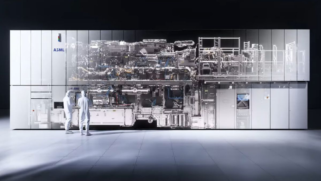
This form of light is notably weak and can be absorbed by air or glass, necessitating a vacuum for its travel and the use of mirrors instead of lenses to focus it onto the silicon wafers accurately. In partnership with Zeiss, ASML developed ultra-precise curved mirrors with atomic-level smoothness to achieve this. The fabrication process is so delicate that even a tiny speck of dust can disrupt the patterning of the microchips, which function as transistors.
ASML’s success was a collaborative effort involving support from the Dutch government, which invested nearly EUR 10 billion over two decades in the development of this technology. Additionally, ASML joined forces with US-based Cymer (now part of ASML) for the EUV light source and partnered with Germany’s Trumf for laser amplifiers. The machinery itself comprises 100,000 components and is roughly the size of a typical bus.
The Significance of ASML
Given the challenges involved in EUV technology, even major semiconductor players like Intel and TSMC have opted not to develop their own EUV lithography machines, instead relying on ASML’s products. Furthermore, these companies, along with Samsung, have invested in ASML to expedite its research and enhance its capabilities.
ASML currently holds the distinction of being the sole manufacturer of EUV lithography machines globally, pricing each unit at about EUR 350 million (approximately Rs. 3,480 crore). While Canon and Nikon produce DUV lithography machines, neither has ventured into EUV technology, creating a monopoly for ASML in providing machines capable of fabricating chipsets with transistors smaller than 7nm.
Technology and Political Tensions
ASML’s unique position has placed it at the center of geopolitical tensions, particularly amid the ongoing standoff between the United States and China. In 2020, US officials exerted pressure on the Dutch government to deny an export license for an EUV machine intended for a Chinese company. Consequently, the shipment was rejected, and the Netherlands continues to prohibit such exports to any Chinese entities.
This escalation prompted China to publicly denounce the Dutch government’s export controls, branding them as “unilateral bullying” and a form of technological suppression. In response, China has initiated domestic efforts to develop similar technologies, although there are currently no reports of success in this endeavor.

